Applicable Standard
IEC 60228
IEC 62067
AEIC CS9-15
Rated Voltage
345(362) kV
Cable Construction
CONDUCTOR
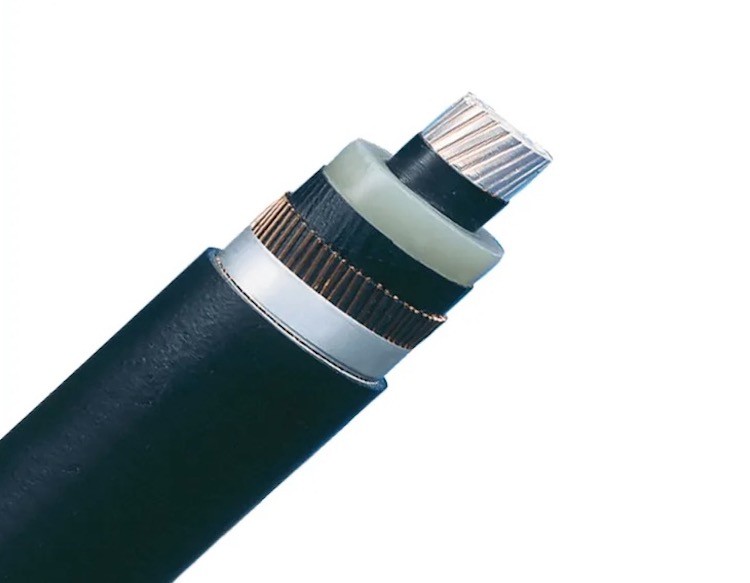
The conductor construction shall be compact class 2 segmental type (Milliken) with circular cross-section made of plain aluminum.
The nominal conductor cross section shall be 2000 mm2, with maximum electrical resistance at 20 °C according to IEC 60228.
The conductor design shall guarantee a maximum skin effect factor of 0.25 and maximum proximity effect factor of 0.15 as per the document “Large cross-sections and composite screens design” issued by CIGRÈ Working Group B1.03, 2005.
The conductor shall be blocked against longitudinal water penetration and shall be approved in the test of annex E of IEC 62067, with exception of the pressure that shall be 35 kPa instead of 10 kPa.
The supplier shall demonstrate the compatibility of the water blocking compound with conductor semiconducting screen materials (swelling powder, tapes, and extruded layer) by means of suitable tests of stability of electrical properties.
CONDUCTOR SEMICONDUCTING SCREEN
conductor shall be free of defects and shall not affect the uniformity of the extruded layer over it.
The minimum average thickness of extruded layer shall be 1.20 mm while the lowest thickness shall be at least 90 % of the average thickness.
The semiconducting tapes shall not impair the longitudinal water penetration test performance.
The extruded layer of the conductor semiconducting screen shall be thermoset and be in contact with semiconducting tapes and fully bonded to the inner surface of insulation under all foreseen operating conditions.
The interface between the extruded layer of the conductor semiconducting screen and inner surface of the insulation shall be uniform, continuous, without micro voids, concentric and smooth. As a reference for optical examinations, no protrusions, or irregularities higher than 30 μm are acceptable.
The semiconducting extruded material shall be super smooth and have sulfur and ash content lower than 0.005 % and 0.01 %, respectively.
The maximum electrical resistivity shall be 1000 Ωm, measured according the test of IEC 62067, annex D.
INSULATION
The cable insulation shall be extruded simultaneously to the conductor semiconducting screen and insulation semiconducting screen using a true triple extrusion process.The insulation system shall be dry cured under pressure. The degree of crosslinking of the extruded insulation shall be 100 %, with no traces of remaining peroxide.
The insulation shall be free of micro voids and contaminants.
The degassing process after extrusion shall effectively remove crosslinking by-products and not cause deformations in the insulated core.
The nominal thickness of the insulation shall be designed for 40 years life to withstand the stresses due to:
a) Electrical alternating voltage operation, including periods at maximum operating voltage
b) Electrical lightning impulse voltage of 1175 kV
c) Electrical switching impulse voltage of 950 kV
d) Thermal aging at normal operating temperature
e) Thermal aging at emergency operating temperature
f) Thermal effects of short circuit temperature
In addition, the electrical stresses at outer insulation surface shall be compatible with commercial accessories with good testing and field performance.
The manufacturer shall supply test data and calculations supporting these design and reliability requirements as required in clause 9 of this specification.
The lowest measured thickness shall not fall below 90 % of the nominal thickness.
The insulation shall overcome the following tests of IEC 62067 and IEC 60811
a) Tensile strength and elongation at break without aging
b) Tensile strength and elongation after aging in air oven
c) Tensile strength and elongation after aging of the complete cable for checking compatibility
d) Hot set test
e) Shrink back according to IEC 60811
INSULATION SEMICONDUCTOR SCREE
The extruded layer of the insulation semiconducting screen shall be thermoset, and fully bonded to the outer surface of the insulation under all foreseen operating conditions.
The interface between the extruded layer of the insulation semiconducting screen and the outer surface of the insulation shall be uniform, continuous, without micro voids, concentric and smooth. As a reference for optical examinations, no protrusions, or irregularities higher than 50 μm are acceptable.
The minimum average thickness of extruded layer shall be 1.20 mm while the lowest thickness shall be at least 90 % of the average thickness.
The maximum electrical resistivity shall be 500 Ωm, measured according the test of IEC 62067, annex D.
One or more semiconducting tapes shall be applied over the extruded layer as a bedding to prevent deformation or indentation of the outer part of the insulation underneath.
CABLE MARKING
The oversheath of each cable length shall be marked at every meter with the following information:
a) Cable cross section (2000 mm2)
b) Materials (Al/XLPE/Cu/Al/HDPE)
c) Nominal voltage 345 kV
d) Name of the customer
e) Date of manufacturing in format day/month/year
f) Sequential length in meters
g) Traceability information code
The traceability code shall be agreed between supplier and purchaser and contain at least the sequence of insulating core extrusion runs.
The characters height and color shall be clearly visible at naked eye. The characters shall resist to abrasion and sunlight during installation.
